Progress is still being made on the exact modifications to be made to the video bios to get perfect picture in all video modes, so in parallel I am working to finialize the flashing patch so removal of the flash chip for programming is not required.

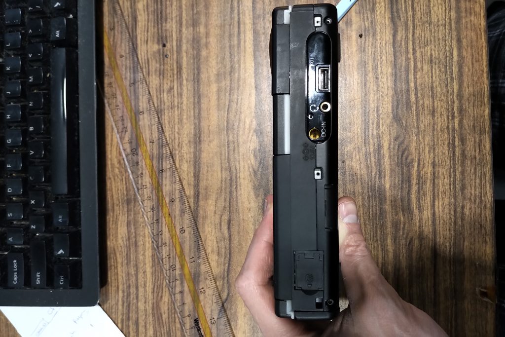
Currently to enable Vpp 12V for programming (pin11) I need to execute a sequence of read/writes to i/o addresses FC23h, F023h, C023h, 23h, 24h, 25h. The sequence was determined from disassembly of xpatch.exe

Update:

So the initial instructions on 23h do in fact seem to be an unlock sequence, and 24h,25h appear to be index and data registers. I had this feeling as xpatch was reading the values but doing nothing with them, so I started searching for the values with “unlock”.

https://patents.google.com/patent/US5630052

The above patent document basically confirms the concept of four consecutive reads, to FC23,F023,C023,23 to unlock/enter a configuration type command. So this is some progress, it is good to know these do not have any special meaning. This may be common knowledge people who work on these systems often.

So this leaves to do more investigation on the 24/25 index/data registers, and actually to understand what is this even commanding, the VLSI chip or the CPU. I am in the process removing the BGA packages from a board and tracing the wires out.

I want to understand their exact purpose of each register and not “guess”, however the datasheet for the VL82C420FC5 “SCAMP” (Single Chip At Mid Performance) is not available so I continue to read similiar datasheets for individual VLSI components to understand the methodologies and interfaces.

Video Bios

The attached vpatch.c does not include the flashing routines, it requires more testing. This simply updates the bios in memory which is useful for testing the XR values to get it tuned in exactly where we want and verify functionality. Unfortunately I do not believe you can enter easy setup from a warm reboot.

When the program is run it checks to make sure the bios in memory is what it expects, and then changes the required values. A reboot (ctrl-alt-del) is required for the video bios to re-run its initialization routine. I do this as I am simulating if the flash had been updated. To make this a functional temporary patch it would be possible to set the XR values in the CT65535 registers on the spot as well, or potentially re-call the initialization routine.

The changes will stay in memory until the power is reset or a hard reboot / jump to FFFF:0000 occurs.

PCB

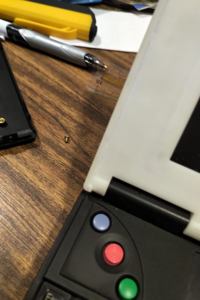
I am using my V3 PCB for testing. I have not modified the 3D printed bezel yet so it cannot fit flat as there is not quite enough space so I have just glued it standing up for testing and cut the window as needed.

I want to be sure the DC-DC I have selected is suitable before spending more time on the mechanical aspect of fitting it. I had one fail, the output capacitor failed to a short. This burned out the 630mA fuse on the PC110 inverter board.

On the next revision of the board I will be including a fuse below 630mA to try and prevent any faults in the TFT retrofit blowing the PC110’s inverter fuse as it requires the entire unit to be taken apart to properly replace it.

I currently have the onboard PIC10 set to control a fixed 5% backlight brightness while I investigate the DC-DC’s and what an acceptable max brightness is.

Trial Run Modified Bios

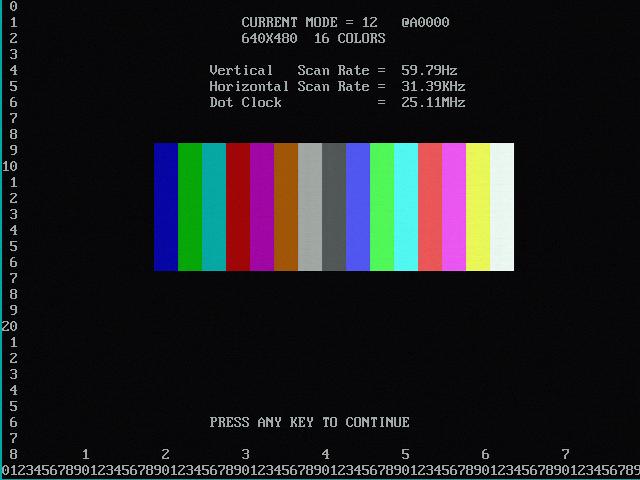
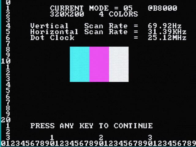
Here is a test run with a bios modified and programmed outside of the PC110 to demonstrate the end goal. The screen is not properly aligned as there are still a couple registers I need to properly update.

This is the preliminary design for the V3 PCB. I will update this post with better details tomorrow. I noticed some not so nice routing I need to fix/clean up.

Summary:

  • Support for AT050TN23v1 display module only
  • Take power from the inverter connector
  • Uses PIC microcontroller to generate the PWM signal for the LED backlight intensity based on the level of the constrast/lcd driver output (Fn-Ins/Del)
  • Resistor values will be confirmed later. if needed the MCU program can “learn” the minimum and maximum voltages to give the best resolution possible.
  • Uses the premade DC-DC converters that are mounted on the back, I don’t think noise will be an issue.

This is version 1 of the prototype. I will add some section to support the metal components, because they are flexible and slightly bent they are not close to the outside, so it makes it hard to put the screws in when closed. I will add a section that forces the metal to be straight and ready to accept a screw.

This SLA of course is not dyed and no surface finishing work has been done.

Update: Here are the files for this attempt:

These are the brass press inserts I used:

https://www.mcmaster.com/94510A360/

This is the initial design for the prototype bezel to hold the ZJ050NA-08C

There are some challenges with 3D printing due to how thin some areas are. I expect to receive an SLA print of this on this coming monday, and from there I will look at additional revisions and print another one until it is just right.

With some surface finishing I hope we can get it close to looking factory, but certainly it will be functional from a mechanical perspective.

I continue to work on various aspects of the PC110, but updating information online in of itself is a task!

Bios Patcher
I continue to work towards understanding the method xpatch.exe uses for updating the flash memory, with the goal of creating a “vpatch” which will make the required modifications to the CT65535 bios for use with the TFT display. I will not get too adventurous until my ZIF sockets arrived so I can easily repair the flash program in the event an early version of vpatch “bricks” the unit.

I am using a combination of Turbo Debugger and Ida to understand and follow the actions. I was unable to find documentation for the VLSI VL82C420FC5, however I did find one for the VL82C480, and it appears that many of the configuration registers must have been shared between them.

TFT Display

I have put the AT050TN22 V.1 on the shelf for now, it seems to be very sensitive and not electrically compatible with the PC110 without some further electronics, perhaps some kind of impedance matching, this is something I do not know enough about right now to deal with properly.

The ZJ050NA-08C however works almost perfectly without any special conditioning of the signal lines. I had a slight issue with blue, it may have been a solder bridge or an error in my PCB, I will address this in the next revision of the board. There are some mechanical changes now needed as the ribbon cable location is changed, and the analog power and backlight requirements are different.

This was the concept V2 PCB but it will be totally different for the new display. Of course I had mixed up the footprint of the 30pin connector which is why it does not go in the correct direction.

Bezel
I spent some time in Fusion 360 drawing the bezel, however I just do not have the time to do this properly so I am going to go back to my original plan and find somebody local to draw it for me.

I got quotes for injection molding tooling, and it would be around $3000. If 3D printing cannot produce a good enough result, this may be the only way to get a professional result. I would need to sell additional pieces over time to recover that cost. Maybe $50 dollars each or something.

Keyboard/Mouse Dongle
I managed to find the propritary keyboard/mouse dongle online so I will be able to look closer at the possibility of 3d printing a custom 1mm pitch housing and using other JST or other style pins to fit into it.

I have done this previously, but this another run with the AT050TN22v1 and its matching VGA driver connected to the external VGA of the PC110 docking connector. Display is slightly cut off because the screen is just in there temporarily. This just to remind myself and demonstrate again that the screen is in fact okay and has good contrast and can properly display all the colours.