As is customary with all my hobby projects, completion is illegal, so I look for improvements and additions.
Unable to fall asleep, I decided to take a break from scrolling twitter and play on the PC110. This is when I realized, of course, the keyboard is not illuminated and I could not type. So I wondered, can I integrate a light onto the lid as I have had on previous thinkpads.
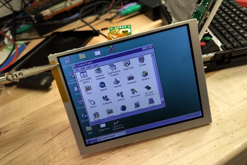
The screen actually looks good. You can see the uneven backlight because I have it turned up quite high, showing an all black screen, in a dark room.
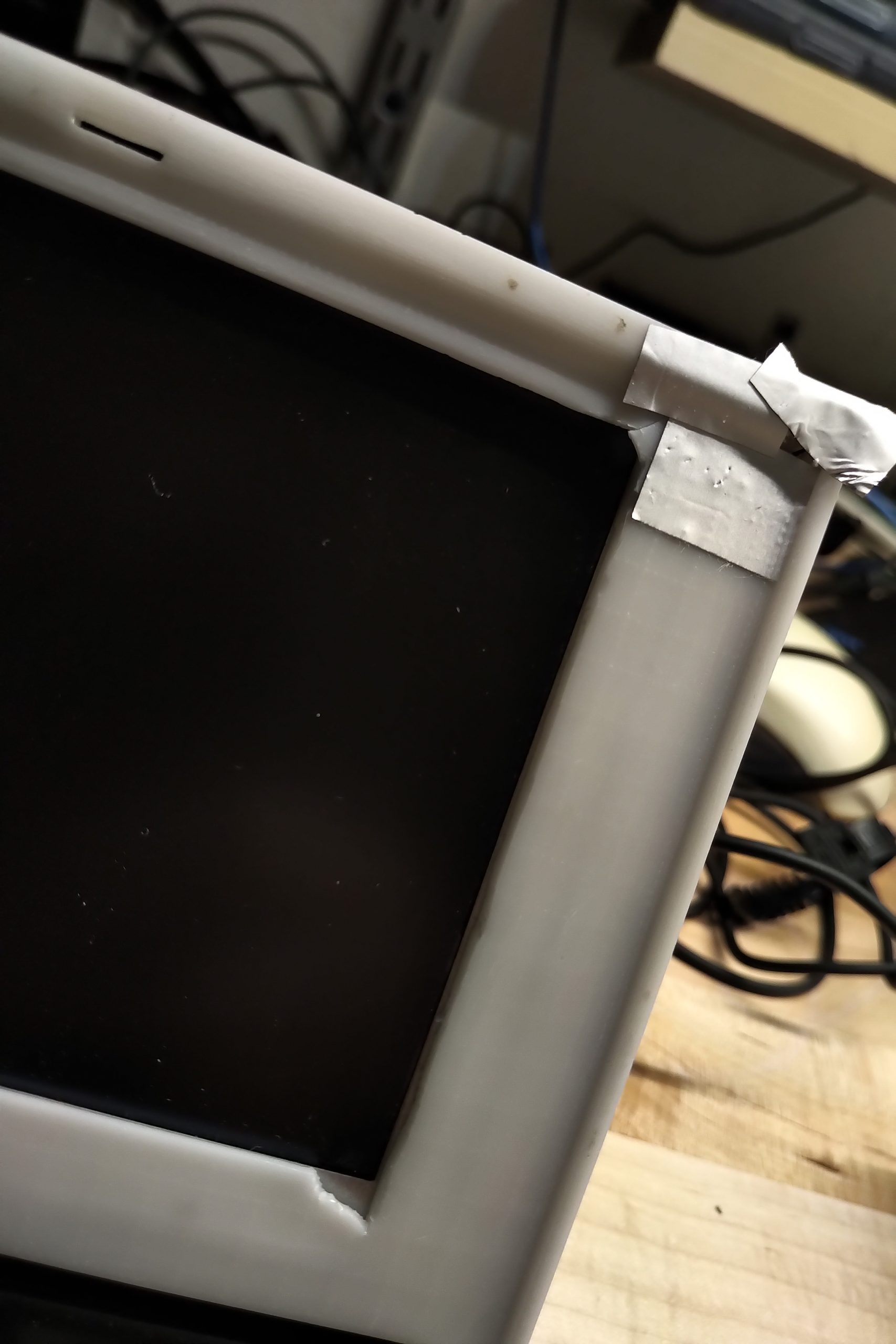
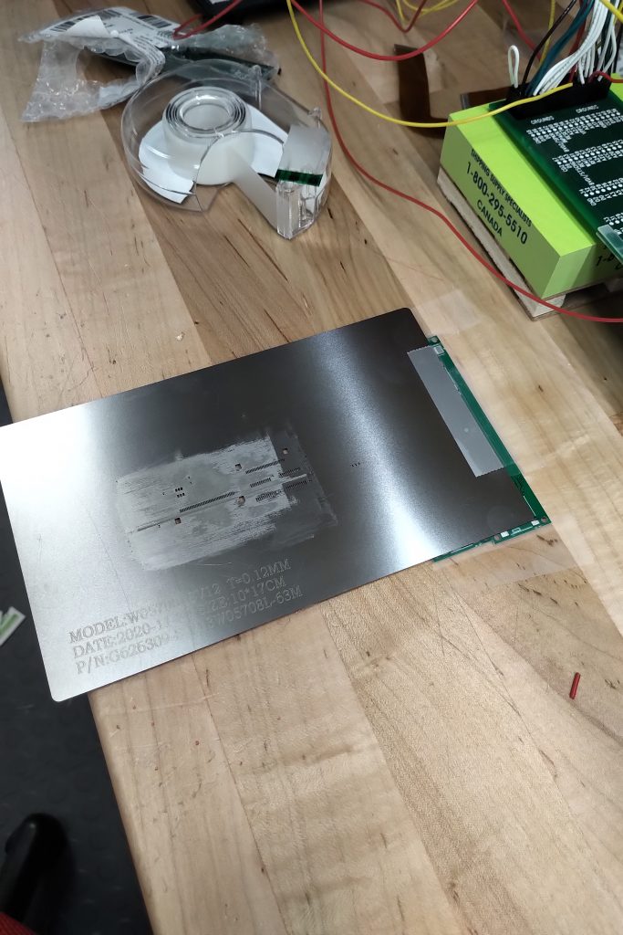
I have the shielding tape because the unpainted plastic was getting illuminated by the light as well from behind. If I move ahead with this, it will most likely have to go on the corner as space is very tight in the middle due to the latch.
I played with placing it other places further down near the keyboard, and while that can work it it would be difficult to conceal.
As I mentioned in my video, it is currently blue as I burned out the only white 0603 LED I had on hand, but I lots of red and blue from a previous project.
I will also thing is a nicer way to control the brightness of the display and toggle of the keyboard light, make sure i am making the best use of the limited options.
Up until now, to use a TFT display on the PC110 you need to run a program after boot. The original method is running CT65535.exe from Taka that updates the CT65535 registers as required which mostly works well except some XR values can be overwritten if you switch LCD/CRT with the Fn-Key and potentially some mode changes can cause unexpected issues. I then implemented an alternate method that updates the video bios in shadow memory and soft reboots. This method is almost as if the settings were from the factory and allows use of the Fn- key for CRT/LCD and ensures that it will work in all modes, however you still cannot enter Easy Setup and the change is lost on hard reboot. It was not much of an advantage over CT65535.exe, but the method of patching the binary bios image itself was a necessary step leading up to this flash updater.
Now that I have successfully managed to update the flash memory, I am able to apply the modifications directly which now allows full use of the system even Easy Setup.
I still need to do some additional work before I can make it available
Check that A/C power is connected and Battery is fully charged
Verify the bios is an expected bios
Check that no TSR is loaded that can interrupt the process.
Provide command switches to specify VGA-TFT, WVGA-TFT, DSTN (Origional)
Here is an idea (I had early on and remembered today), whereby if you change the brightness quickly multiple times within 2 seconds, it enters into a “custom” brightness mode. I flash the display 3 times to let you know that this mode has been entered.
A reminder why this could be useful. The PC110 allows three brightness levels, but only two when on battery power. So this would be way to access everything from the minimum 1% to the maximum 100% even while on battery power, if you are not satisfied with the default levels.
I will update the program to have a timer so the brightness of the display does not actually change until no key has been pressed for maybe half a second to avoid the display changing brightness while you are trying to enter “custom” mode.
I still need to take some measurements on current consumption vs light output to decide what the ideal low/medium/high values should be, and what “custom” levels should be included.
Power Default Levels
milliWatts
Luminosity
Low
10%
137
Medium
50%
809
High (A/C Power Only)
100%
1670
Custom Levels
1/10
0%
0
2/10
2%
32
3/10
8%
147
4/10
16%
263
5/10
24%
399
6/10
32%
536
7/10
48%
798
8/10
63%
1061
9/10
79%
1313
10/10
100%
1670
I obtained the above power measurements by powering the PC110 from a bench power supply at 10.5VDC. The baseline power consumption was 4000mW with no battery installed and the screen electronics energized but the backlight off. With full backlight on the total consumption was 5600mW.
By comparison the OEM display consumption is 1418mW at low, 1733mW at medium and 2205mW at high.
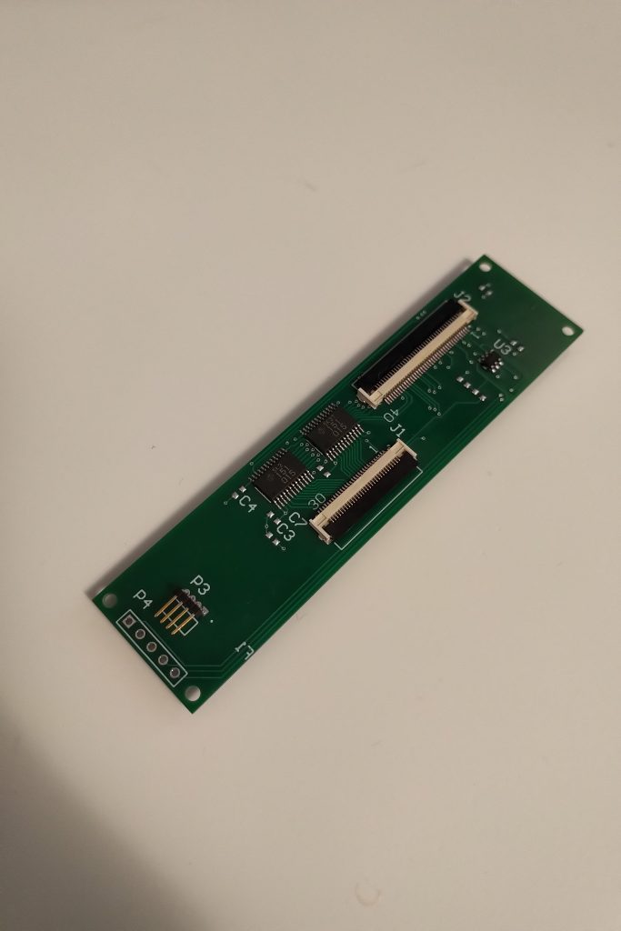
In the previous design, I was reading the voltage of PIN3 of the PC110 30pin connector which is the original LCD driving voltage. It’s range is about 22V to 30V and is controlled by the contrast keys in I believe 256 steps. I was using two resistors to form a voltage divider to bring 30V down to ~3.3V for the ADC of the PIC. The problem is, it can take quite some time to go from 0% to 100% contrast and even still this only provides a voltage range of ~2.4V to ~3.3V, and the resolution of the ADC is low so the noise is a problem. The intention had been to have more than the standard (3) brightness levels, however in practice this methods is only useful if a high resolution ADC was used or other analog circuity was put in place to better scale the signal.
I have revised the PCB to instead use the original brightness signal located on PIN3 of the inverter wire.
I have placed a 10kohm resistor from PIN3 to Vcc (3.3V), and the below measured voltage is as measured at Pin3.
Intensity
Pin3 Ohms to GND
Measured Volts
ADC
Threshold
PWM%
Low
25k
2.75
213
<255
1%
Medium
10.5k
1.75
135
<150
50%
High
5.4k
0.75
58
<100
100%
The low and medium brightness is TBD, I will try to select the optimal values to pre-program.
High brightness is only available while connected to A/C. Although the PC110 has no issue providing the current for the LED backlight, it may have been designed to restrict full brightness on A/C because of the higher draw of the CFL backlight inverter.
Either way, the brightness between medium and high will not but massive in terms of light output, so it can be considered with this was you can switch between the lowest brightness, and the ideal brightness.
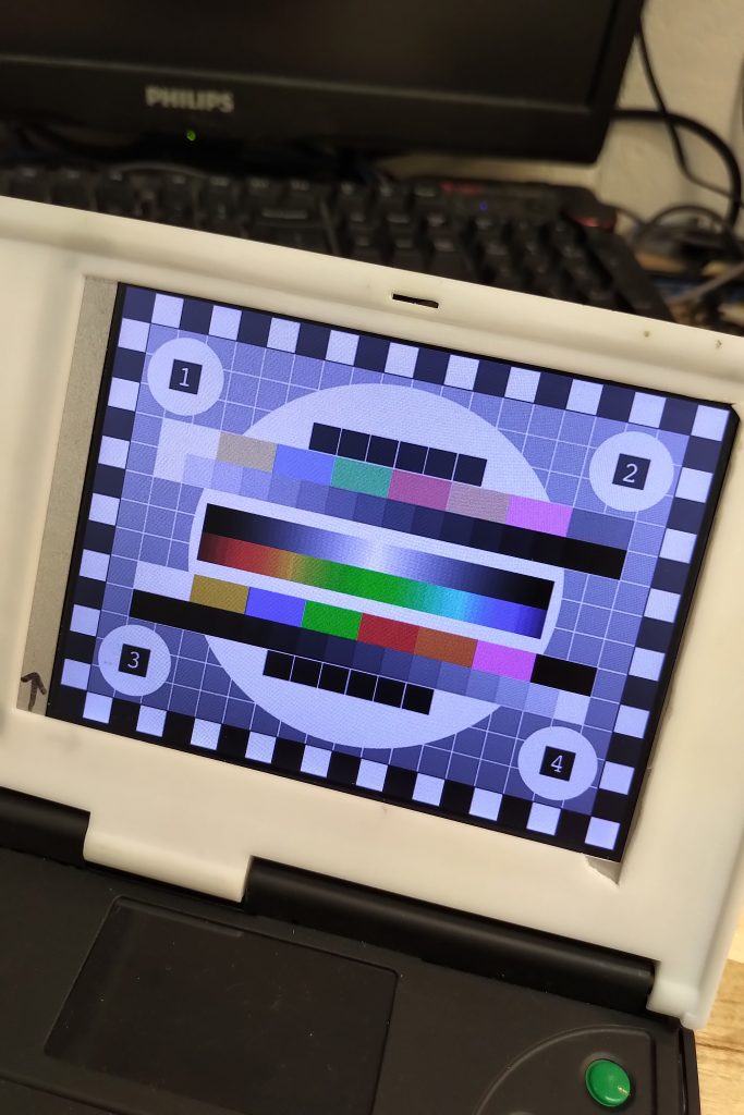
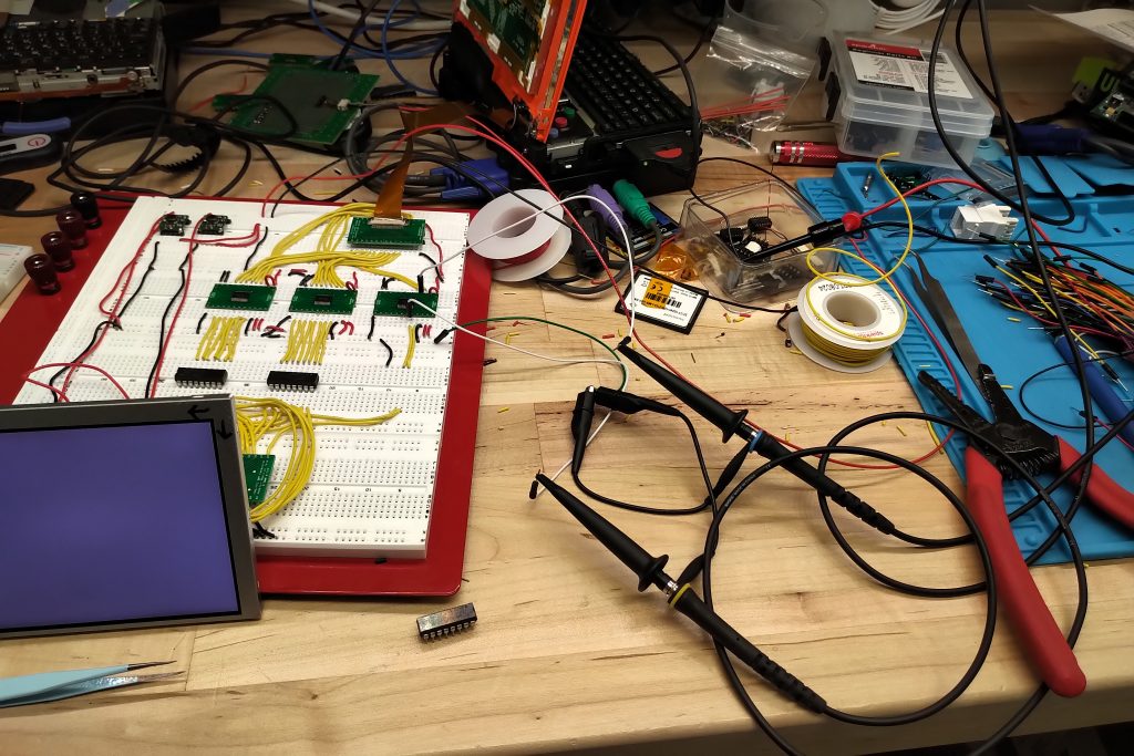
This is revision 2 of the bezel. It fits quite well, there are some additional changes I would like to make in relation to the fitment. The top might look slightly loose as I did not put in the metal plate for the upper latch as the hole is slightly misaligned and I need to fix it.
I am currently using an additional blank PCB and pieces of a PCB as retention clips for the display, while I decide if I should make a single retention piece that attaches to all of the standoffs to add rigidity, or just make small tabs.
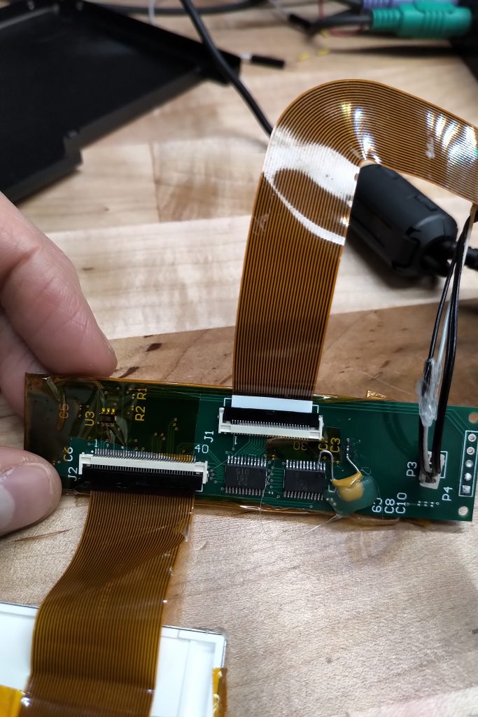
As well the latest version of the PCB that is due to arrive later this week slightly moves the position of the connector to make the 30pin ribbon came lay more naturally without any tension when the back cover is on, although even how it is now is no issue. In fact I hope I have not moved it too far as this feels good compared to when I had the PCB hot glued into place on the previous hand modified prototype “1.5”.
I will also paint the interior of the bezel under the PCB with conductive paint to shield emitting noise.
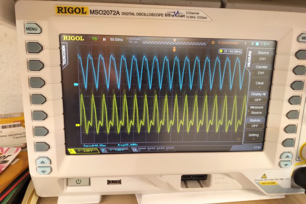
The issue I described as “blue tint” turns out to have been a fault in my test system. I built another revision of the PCB including pads for capacitors, and it would seem I only needed to place a cap on the clock line to resolve the remaining signal integrity issues.
Current Status
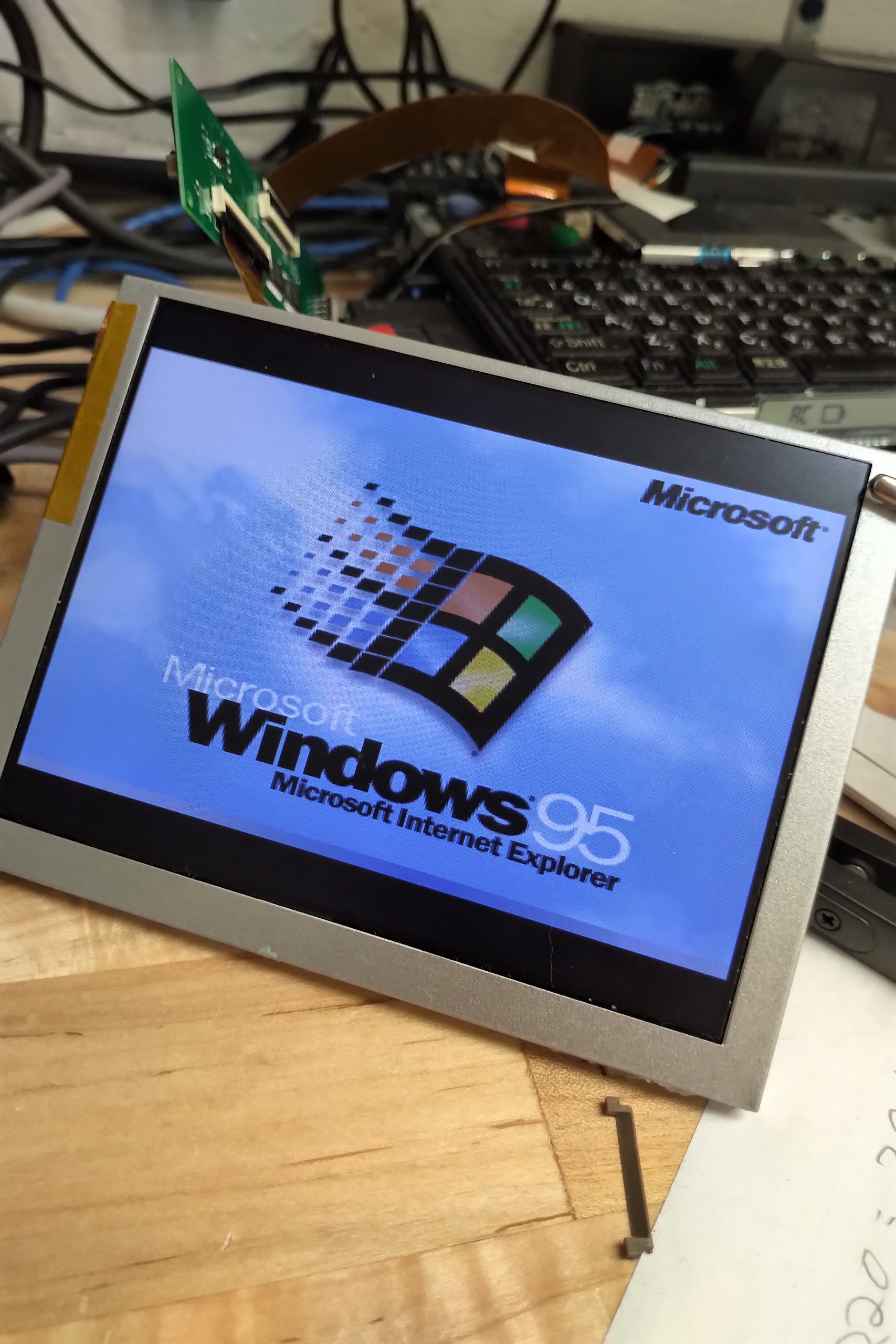
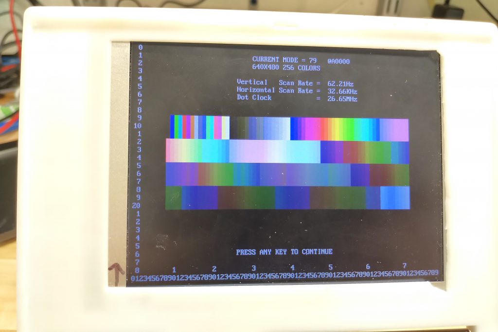
Full VGA Clock (25.175MHz) without any pixel errors / artifacts
Full brightness control via the contrast keys
Less than 100µA draw on the 10.5V inverter supply while display is off.
All electrical load is on the inverter supply wires and not the fpc.
250mA fuse to reduce risk of blowing the internal 650mA fuse in any unexpected failure modes.
Using the Hitachi transceivers maintains same electrical interface to the CT65535 as the OEM display. This may be an overkill step but it is working well so I am sticking with it.
Next Steps
Further verify there are no pixel errors at the higher clock speed.
Revise the PCB to simplify assembly and clean it up.
Update the 3d model for the new bezel to accommodate the new PCB.
This is just a quick update. This is more a journal to myself and as always I most say I do not know what I doing generally, so consider this as entertainment more than information.
TLDR: I have had some success using the Hitachi level converters and terminating capacitors. I believe this issue is all about transmission line theory, which I am aware of but do not understand so this is trial and error. I am ordering another revision of the board this week and starting to try and finalize the 3D model for the bezel.
I do still notice a blue tint in certain mode tests, I am not certain this is a hardware issue yet I need to investigate it more once these other issues are sorted out.
I continue to chase the goal of being able to drive the replacement display at the full VGA clock speed of 25.175MHz / ~60hz refresh rate.
To summarize the issues I have been facing, in various versions of the PCB’s and hand wiring there was noise, jitter and other timing issues visible when certain patterns were displayed on the screen. The effect was not as bad when running at 15MHz but still there. It was terrible with sloppy handmade boards and breadboard testing.
I attempted to fix this with various forms of shielding, however it became clear the the issue was not external noise, and the reason the the metal back plate improved the situation was due to some kind of inductive coupling or similar effect on the ribbon cable.
I concluded the issue was related to an impedance mismatch causing reflections of the signal. I looked at what type of source termination and receiver end termination may have been in place.
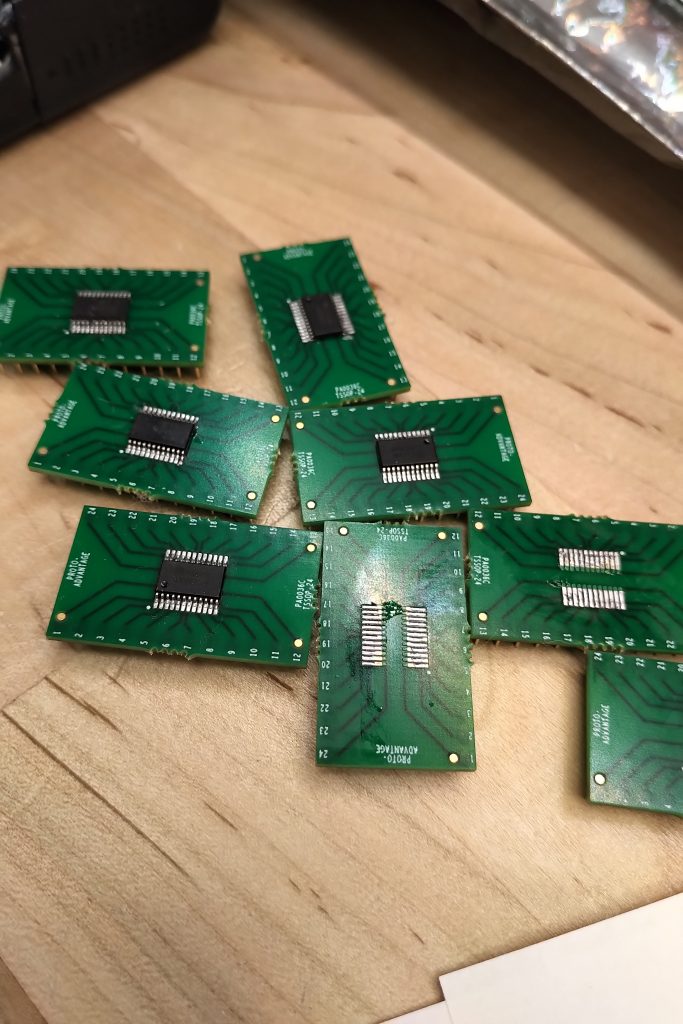
I found that all signals including the clock appear to have a 0ohm resistor between the CT65535 output pin and the FPC connector, and they are each coupled to ground with a 50pf or so capacitor. On receiving side they went straight into a Hitatchi HD151015 9 bit Level Shifter / Transceiver.
I figured these values and topology were designed based on the length of the path from the CT65535 through to the CSTN at the original clock speed (~8mhz if i recall).
Of course this is no longer the case with the adapter board where two new connectors are introduced, the traces on the adapter PCB, the ribbon cable on the AT050TN23v1 and then the difference of the input gates/etc on the TFT.
I had various attempts at implementing signal termination at the converter PCB and on the TFT DCLK pin itself with varying success but nothing repeatable. What would work with test leads would not work once soldered on. What worked in one orientation would not work in another it was all random. I believe this may have at least in part been related to trying to terminate in the middle of the transmission line and not close enough to the end.
It had also been observed that lowering the voltage of VCC on the TFT could improve the issue slightly, this was not practical but got me thinking about level converters to address the flight difference the PC110 ~3.5V and the 3.3V of the DC-DC. I also knew that the immediate input on the OEM display was a Hitatchi level converter.
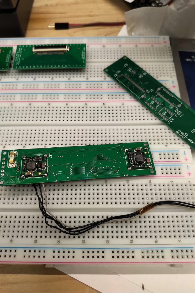
I purchased every possible level converter I could find on digikey, and generally the results were identical to it not being used at all. I then tried harvesting the Hitatchi level converters off an old CSTN and suddenly the signal was drastically improved, but still had some issues which I assumed was related to the hand wiring used for testing
I produced a PCB to properly mount the Hitachi chips and upon initial testing there was almost identical issues with the signal/display as without the Hitachi chips. This was starting to solidify a sense of defeat.
Due to missing (still missing) digikey delivery I was without the various capacitors to mount on the board, so there was still a small hope that the bypass capacitors on the level converters could help but not likely.
I then thought again if the previously attempted termination methods that failed would now have better luck given the long transmission line from the PC110 was now being terminated into the Hitatchi chip. Magically now, coupling the clock signal to ground with a 100nF capacitor at the input to the Hitatchi made the signal essentially perfect. Although I have not found issues yet, I expect there may be test images that result in some individual signal lines approaching clock speed and can benefit from the same filtering. Now I understand the issue is more about the speed of the transmission and not the frequency itself, but in practice it seems to be related to the frequency in this case.
I am going to order another revision of the PCB that will place 100nF capacitors as close to the Hitachi pins as possible. It is possible this approach may work with other actively available level converters but given the low volume of this project harvesting hitatchi chips from old displays and/or purchasing some limited qty of new old stock is good enough. It is also nice that the Hitachi chip has 9 channels allowing to accomplish the task with two chips, whereas most of the new parts are only 8 channel. The board is tight and my routing skills are limited.
Again in closing, I believe this all falls within “transmission line theory”, and with proper understanding it may be possible to simply place series resistors and/or capacitors on the converter board and with a correct value and solve the problem with less components i.e. no converters.
I am however taking the route of using the level converter chips to deal with the fact there is a difference between the Vcc from the 3.3V DC-DC and the “3.3V” on the PC110 motherboard. Putting the capacitors on the signal lines should create an RC filter, but I am not putting a resistor as I am assuming (from experimental testing) that the resistance of the trace/gate/etc is acceptable.
I am still trying to figure out what to do with the all of the signals but the clock signal in particular is of concern. It seems that the integrity of this signal may be the main cause of the distortion seen when running at 25.175MHz and even some at 15MHz. The distortion can be as simple as a single pixel shadow to the right on a black screen, or in more severe cases it appears as “jitter”. Previously we have attempted to compensate for this by lowering Vcc on the TFT display to try and have it handle the poor signal levels due to the assumed reflections. This signal integrity issue exists on all the signals, but the clock is the worst which is why I spent some time focusing on it. Maybe correction of it alone is not enough. Do I need to put level shifters/buffers onto the PCB?
I do not know what I am doing here, so if anybody knows better please help!
My measurement technique is almost certainly not correct and will be a contributing factor to the deformation/distortion of these measurements.
As we are looking for a solution that does not involve any modifications to the PC110 itself, there are only
Clock Speed
PCB Routing
Bus Transceiver
End Termination
CT65535 Drive strength paramter (XR6C bit2)
Clock Speed
One complete frame is 525 lines. Each line is around 800 clock ticks. That means about 420k clock ticks per frame. So at 25.175MHz the refresh rate is around 60hz. At 15MHz it is closer to 35Hz. My goal is 25.175MHz still.
PCB Routing
I already have the trace quite short, however I think I can do better to reduce the sharp edges and surround it better with grounds. I will do more reaching on this and try to look at other designs for examples.
Bus Transceiver
Maybe this is too complicated and not needed, but maybe it is needed to use a voltage level translator much like what is found on the citizen board. I could place three of these 8 channel chips to handle all signal lines, so no longer a need to worry about the voltage difference between the PC110 “3.3V” and the TFT’s Vcc, as well the signal is regenerated.
Termination is a complex topic for me. I have no chance to calculate what is needed so it will be trial and error. I am contemplating how to place the appropriate pads to allow experimentation the potential termination methods (single parallel resistor, RC, Thevenin, Schottky diode) etc, but without further aggravating the issue of reflect with all those little unused pads.
I already experienced this issue, where I found a nice combination of capacitors (through trial and error) that made the signal perfect, however I was testing with long wires, when I then put the components onto the TFT it did not work because the situation was totally different without those long wires.
Depending on the termination choice taken, maybe it will be needed to increase the drive output of the CT65535 via XR6C bit 2.
Citizen Display Attached
Although waveform doesnot look ideal, you can see at least that the reflection is not so serious and it is close to 3V Vpp with minimum at 0.
The following is the clock waveform measured as it exits the hitachi level shifter on the CSTN control board.
No Connection
This is what it looks like with no display attached
AT050TN23v1
This is waveform with TFT attached.
PC110 DRIVING SIDE
The digital clock output from the CT65535 (Pin B8) connects to the LCD output connector Pin29 via a 0ohm jumper, and is coupled to ground with a 50pf capacitor. I would suspect the 0ohm jumper was a provision for driver side termination? there is no trace running under it so it was not for routing purposes.
On the Citizen display all signals are fed into level shifters.
The following is an updated version of the experimental vpatch. It reads from a config.txt for the values to update in memory, this is to make it easier to verify which values need to be updated without rebuilding the program every time.
the first line is a checksum, if you set it to 0 the program will not check and will update and reboot every time. If you set an expected checksum, it will only update/reboot if that matched, which is good for putting in autoexec.bat
the program has very limited error checking and very simple parsing of the config file so you have to be specific.
this program is the precursor to flashing the chip.