The following is an updated version of the experimental vpatch. It reads from a config.txt for the values to update in memory, this is to make it easier to verify which values need to be updated without rebuilding the program every time.
the first line is a checksum, if you set it to 0 the program will not check and will update and reboot every time. If you set an expected checksum, it will only update/reboot if that matched, which is good for putting in autoexec.bat
the program has very limited error checking and very simple parsing of the config file so you have to be specific.
this program is the precursor to flashing the chip.
Progress is still being made on the exact modifications to be made to the video bios to get perfect picture in all video modes, so in parallel I am working to finialize the flashing patch so removal of the flash chip for programming is not required.
Currently to enable Vpp 12V for programming (pin11) I need to execute a sequence of read/writes to i/o addresses FC23h, F023h, C023h, 23h, 24h, 25h. The sequence was determined from disassembly of xpatch.exe
Update:
So the initial instructions on 23h do in fact seem to be an unlock sequence, and 24h,25h appear to be index and data registers. I had this feeling as xpatch was reading the values but doing nothing with them, so I started searching for the values with “unlock”.
The above patent document basically confirms the concept of four consecutive reads, to FC23,F023,C023,23 to unlock/enter a configuration type command. So this is some progress, it is good to know these do not have any special meaning. This may be common knowledge people who work on these systems often.
So this leaves to do more investigation on the 24/25 index/data registers, and actually to understand what is this even commanding, the VLSI chip or the CPU. I am in the process removing the BGA packages from a board and tracing the wires out.
I want to understand their exact purpose of each register and not “guess”, however the datasheet for the VL82C420FC5 “SCAMP” (Single Chip At Mid Performance) is not available so I continue to read similiar datasheets for individual VLSI components to understand the methodologies and interfaces.
The attached vpatch.c does not include the flashing routines, it requires more testing. This simply updates the bios in memory which is useful for testing the XR values to get it tuned in exactly where we want and verify functionality. Unfortunately I do not believe you can enter easy setup from a warm reboot.
When the program is run it checks to make sure the bios in memory is what it expects, and then changes the required values. A reboot (ctrl-alt-del) is required for the video bios to re-run its initialization routine. I do this as I am simulating if the flash had been updated. To make this a functional temporary patch it would be possible to set the XR values in the CT65535 registers on the spot as well, or potentially re-call the initialization routine.
The changes will stay in memory until the power is reset or a hard reboot / jump to FFFF:0000 occurs.
I am using my V3 PCB for testing. I have not modified the 3D printed bezel yet so it cannot fit flat as there is not quite enough space so I have just glued it standing up for testing and cut the window as needed.
I want to be sure the DC-DC I have selected is suitable before spending more time on the mechanical aspect of fitting it. I had one fail, the output capacitor failed to a short. This burned out the 630mA fuse on the PC110 inverter board.
On the next revision of the board I will be including a fuse below 630mA to try and prevent any faults in the TFT retrofit blowing the PC110’s inverter fuse as it requires the entire unit to be taken apart to properly replace it.
I currently have the onboard PIC10 set to control a fixed 5% backlight brightness while I investigate the DC-DC’s and what an acceptable max brightness is.
Trial Run Modified Bios
Here is a test run with a bios modified and programmed outside of the PC110 to demonstrate the end goal. The screen is not properly aligned as there are still a couple registers I need to properly update.
This is the preliminary design for the V3 PCB. I will update this post with better details tomorrow. I noticed some not so nice routing I need to fix/clean up.
Summary:
Support for AT050TN23v1 display module only
Take power from the inverter connector
Uses PIC microcontroller to generate the PWM signal for the LED backlight intensity based on the level of the constrast/lcd driver output (Fn-Ins/Del)
Resistor values will be confirmed later. if needed the MCU program can “learn” the minimum and maximum voltages to give the best resolution possible.
Uses the premade DC-DC converters that are mounted on the back, I don’t think noise will be an issue.
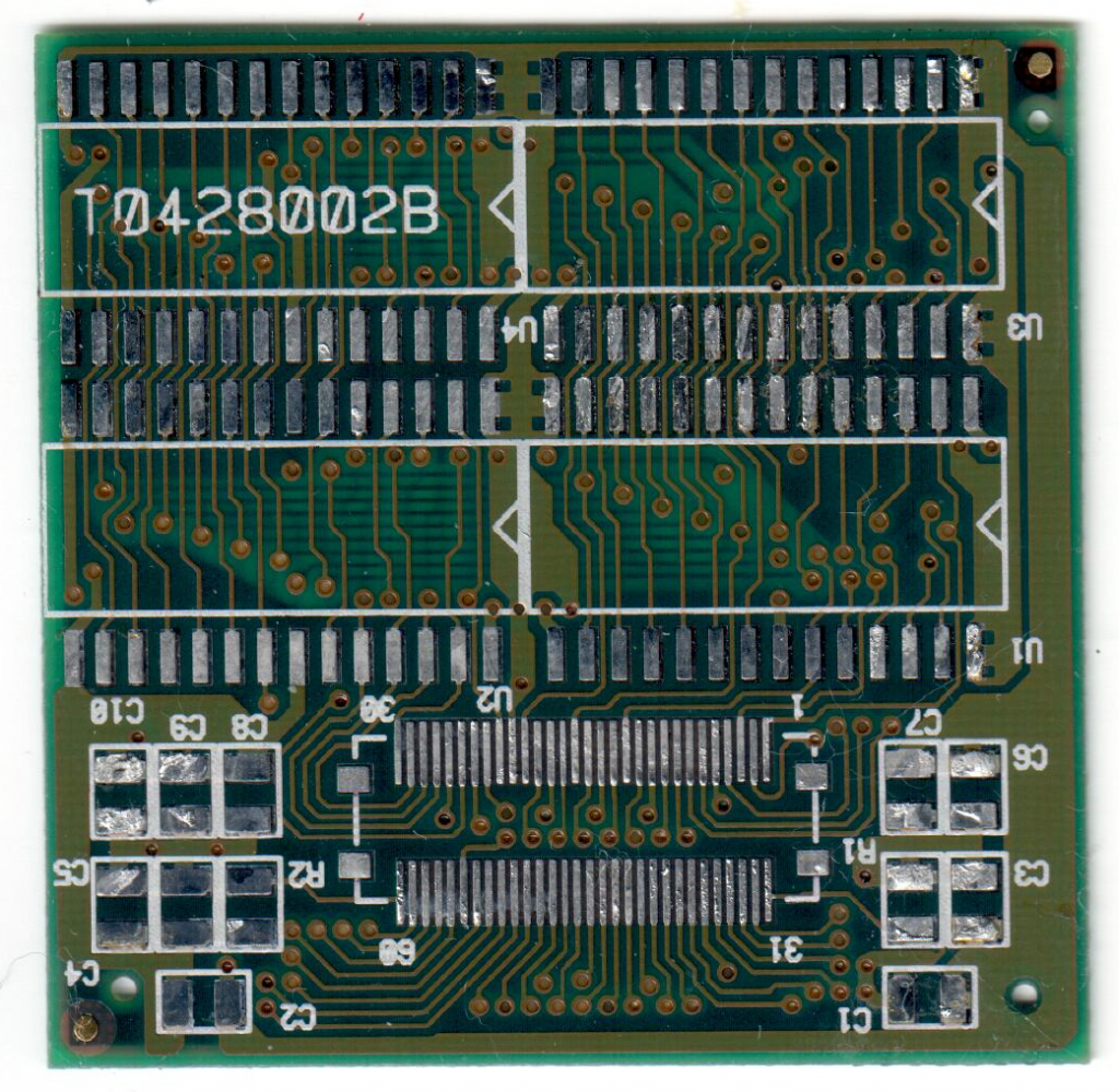
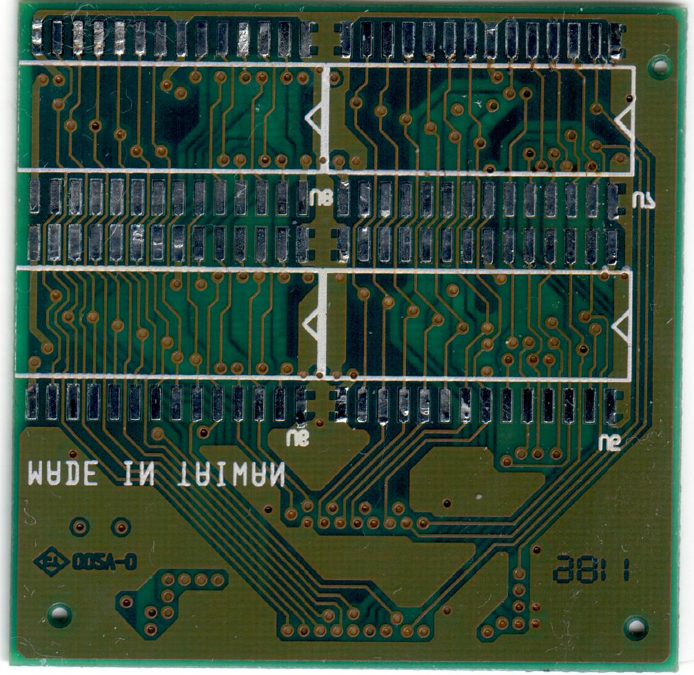
Here are pictures of the PCB for the 16MB module. I will attempt to duplicate this in Altium. PCB Thickness is 0.6mm and is 4 layer on initial inspection.
Connector SideBack Side – Image Mirrored for visualization
In a perfect world, I could buy a bunch of the keyboard/mouse adapter cables and just use regular devices. It is not easy to come by though, so I contemplated making a small dongle to allow pairing of bluetooth devices.
I searched quite a bit and have been unable to find this connector from any of the manufacturers, so perhaps it was truly a custom designed connector style. I was also unable to find it used in any other products, I tried to look at other old products by Ricoh that may have used it including the Thinkpad 220, but no luck.
As an alternative it would have been nice to do the straight PCB method that can be done with USB, however the contacts are recessed on the PC110 so contact would not be made to a flat PCB. What I contemplated was to use a spring contact on a PCB, along with an MCU. This is my proof of concept, mechanically it fits and holds nicely, and the contacts line up and make some contact so I will proceed to investigating what MCU to use and produce a PCB. As a fallback I will put a footprint for a standard ps/2 DIN connector so I could at least use a standard mouse. Not pretty but it will work.
I have done some work with Bluetooth/BLE a while back on another project, but this is new to me. What I need is a chip I can use to pair a bluetooth keyboard/mouse to, and then drive the ps/2 signals. Driving the ps/2 is the easy part, pairing to a mouse/keyboard is uncharted territory for me.