I am a few months late updating my website on this. I designed a prototype board and assembled a prototype board and completed the switchover to a CPLD. Current status I partnered with somebody that specializes in this kind of thing to complete the analog audio design and sort out various details to make it manufacturable. I hope to have more updates on this soon. Below is a video demonstrating the DMA emulation in action, protected mode games and all.
I have not posted anything about this recently, this is one of the other projects I have been playing with. The goal is to create a PCMCIA soundcard that has the following featureset:
Yamaha OPL3 on the expected 388h address (this is done and working)
MPU-401 with full intelligent mode on the expected 330h (this is done and working)
Onboard Dream.fr wavetable general midi chip connected to the output of the MPU-401 (tested and working)
Option to disable onboard wavetable and only use external midi dongle
Gameport on the expected 200h – 207h (working but needs to be optional to enable/disable).
Digital audio via fully soundblaster compatible interface.
There are very few cards that ever existed that provided SoundBlaster support (IBM 3D Sound PCMCIA), and they are near impossible to find for purchase, so it lead me down the path to make one.
The learning curve has been steep as this project covers multiple areas all of which I was unfamiliar with at the start (and am now slightly familiar with). I got a general proof of concept working pretty quickly but spent too much time playing with wav files and large transfers (i.e. sbdiag tada.wav).
My recent reworking of how I was hooking interrupts solved some other issues I was having with protected mode games so I started to do some better testing on Doom,Duke3D etc and this is when I came to realize that they only use 4k or smaller buffers and the actual transfers are 128 bytes or 256 bytes per autoinit cycle. This totally makes sense given the realtime nature of sound effects during unpredictable gameplay.
I currently refill the 4K DSP every time it drops below half-full. This is not going to work. So I need to think about a better way to handle this.
I was avoiding modifying the DSP code, but for no good reason really. I think it is time I modify the DSP code so that my TSR can have complete visibility into how many bytes are being expected during autoinit mode. I am going to think about it a bit.
I am still alive and working on the project, mainly I have been messing around with this idea for the keyboard light, and generally just trying to optimize the 3D model for the bezel.
Something I have noticed is that I can hear a slight buzz from the onboard speaker and headphones when volume is turned up to full and no sound is playing which is most likely originating from the DC-DC converters. I am going to look into that some more and try to cancel that out with some better filtering on the power supply side of things. It seems that even an unmodified PC110 has this noise when the volume is turned all the way up, even with no inverter connected at all.
The BIOS patch is about ready, it works properly I have just been working on proper safeguards (making sure on a/c power and battery is charged etc).
Here is the current revision of the board. I was not paying attention and I ran those traces too close to that mounting hole, not a major issue as the screw goes into plastic and is not tight enough to damage the solder mask, but still not proper I will move it. DC-DC converts of course are on the back as seen in some other photos.
Here is the keyboard light in action, on one of them is working as I broke the other one and I was lazy to deal with it. Maybe only one LED is needed (if any really).
And here is the 3D printed bezel poorly painted just to see if it would block the light (it does). Feels strange without the IBM logo.
And here are just some random pictures working of 3D model progress.
As is customary with all my hobby projects, completion is illegal, so I look for improvements and additions.
Unable to fall asleep, I decided to take a break from scrolling twitter and play on the PC110. This is when I realized, of course, the keyboard is not illuminated and I could not type. So I wondered, can I integrate a light onto the lid as I have had on previous thinkpads.
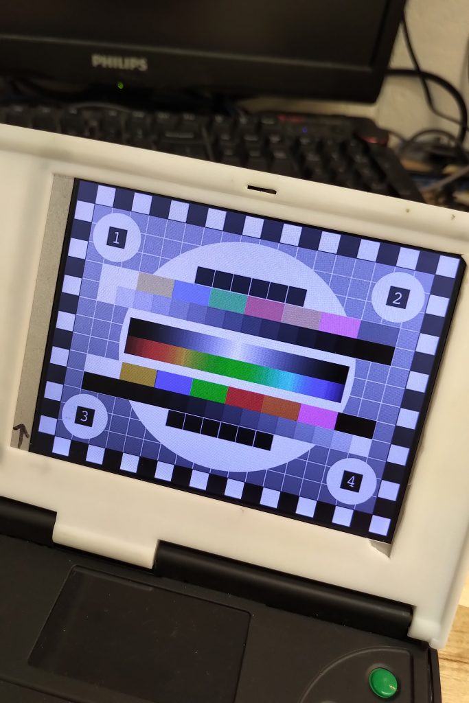
The screen actually looks good. You can see the uneven backlight because I have it turned up quite high, showing an all black screen, in a dark room.
I have the shielding tape because the unpainted plastic was getting illuminated by the light as well from behind. If I move ahead with this, it will most likely have to go on the corner as space is very tight in the middle due to the latch.
I played with placing it other places further down near the keyboard, and while that can work it it would be difficult to conceal.
As I mentioned in my video, it is currently blue as I burned out the only white 0603 LED I had on hand, but I lots of red and blue from a previous project.
I will also thing is a nicer way to control the brightness of the display and toggle of the keyboard light, make sure i am making the best use of the limited options.
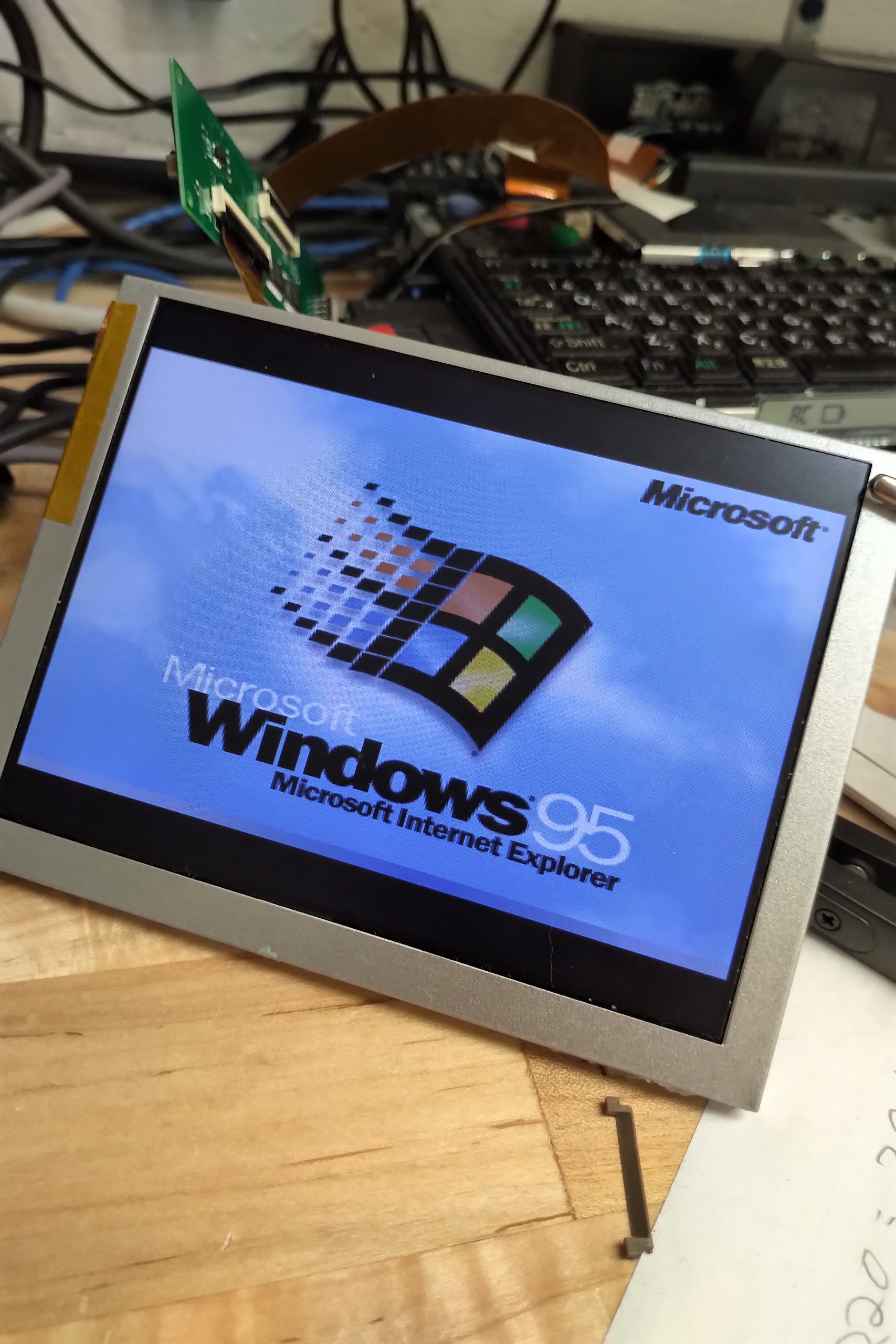
Up until now, to use a TFT display on the PC110 you need to run a program after boot. The original method is running CT65535.exe from Taka that updates the CT65535 registers as required which mostly works well except some XR values can be overwritten if you switch LCD/CRT with the Fn-Key and potentially some mode changes can cause unexpected issues. I then implemented an alternate method that updates the video bios in shadow memory and soft reboots. This method is almost as if the settings were from the factory and allows use of the Fn- key for CRT/LCD and ensures that it will work in all modes, however you still cannot enter Easy Setup and the change is lost on hard reboot. It was not much of an advantage over CT65535.exe, but the method of patching the binary bios image itself was a necessary step leading up to this flash updater.
Now that I have successfully managed to update the flash memory, I am able to apply the modifications directly which now allows full use of the system even Easy Setup.
I still need to do some additional work before I can make it available
Check that A/C power is connected and Battery is fully charged
Verify the bios is an expected bios
Check that no TSR is loaded that can interrupt the process.
Provide command switches to specify VGA-TFT, WVGA-TFT, DSTN (Origional)
Here is an idea (I had early on and remembered today), whereby if you change the brightness quickly multiple times within 2 seconds, it enters into a “custom” brightness mode. I flash the display 3 times to let you know that this mode has been entered.
A reminder why this could be useful. The PC110 allows three brightness levels, but only two when on battery power. So this would be way to access everything from the minimum 1% to the maximum 100% even while on battery power, if you are not satisfied with the default levels.
I will update the program to have a timer so the brightness of the display does not actually change until no key has been pressed for maybe half a second to avoid the display changing brightness while you are trying to enter “custom” mode.
I still need to take some measurements on current consumption vs light output to decide what the ideal low/medium/high values should be, and what “custom” levels should be included.
Power Default Levels
milliWatts
Luminosity
Low
10%
137
Medium
50%
809
High (A/C Power Only)
100%
1670
Custom Levels
1/10
0%
0
2/10
2%
32
3/10
8%
147
4/10
16%
263
5/10
24%
399
6/10
32%
536
7/10
48%
798
8/10
63%
1061
9/10
79%
1313
10/10
100%
1670
I obtained the above power measurements by powering the PC110 from a bench power supply at 10.5VDC. The baseline power consumption was 4000mW with no battery installed and the screen electronics energized but the backlight off. With full backlight on the total consumption was 5600mW.
By comparison the OEM display consumption is 1418mW at low, 1733mW at medium and 2205mW at high.
In the previous design, I was reading the voltage of PIN3 of the PC110 30pin connector which is the original LCD driving voltage. It’s range is about 22V to 30V and is controlled by the contrast keys in I believe 256 steps. I was using two resistors to form a voltage divider to bring 30V down to ~3.3V for the ADC of the PIC. The problem is, it can take quite some time to go from 0% to 100% contrast and even still this only provides a voltage range of ~2.4V to ~3.3V, and the resolution of the ADC is low so the noise is a problem. The intention had been to have more than the standard (3) brightness levels, however in practice this methods is only useful if a high resolution ADC was used or other analog circuity was put in place to better scale the signal.
I have revised the PCB to instead use the original brightness signal located on PIN3 of the inverter wire.
I have placed a 10kohm resistor from PIN3 to Vcc (3.3V), and the below measured voltage is as measured at Pin3.
Intensity
Pin3 Ohms to GND
Measured Volts
ADC
Threshold
PWM%
Low
25k
2.75
213
<255
1%
Medium
10.5k
1.75
135
<150
50%
High
5.4k
0.75
58
<100
100%
The low and medium brightness is TBD, I will try to select the optimal values to pre-program.
High brightness is only available while connected to A/C. Although the PC110 has no issue providing the current for the LED backlight, it may have been designed to restrict full brightness on A/C because of the higher draw of the CFL backlight inverter.
Either way, the brightness between medium and high will not but massive in terms of light output, so it can be considered with this was you can switch between the lowest brightness, and the ideal brightness.
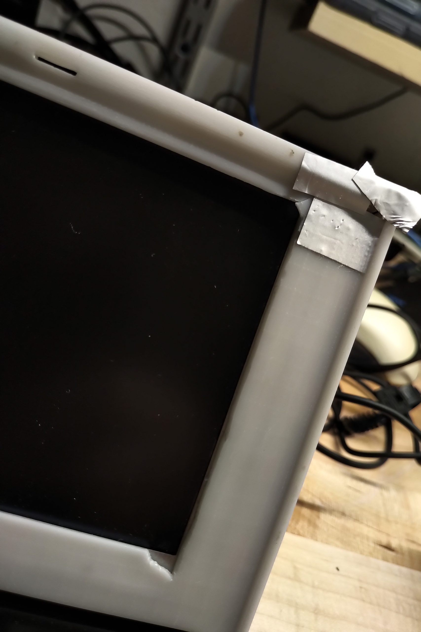
This is revision 2 of the bezel. It fits quite well, there are some additional changes I would like to make in relation to the fitment. The top might look slightly loose as I did not put in the metal plate for the upper latch as the hole is slightly misaligned and I need to fix it.
I am currently using an additional blank PCB and pieces of a PCB as retention clips for the display, while I decide if I should make a single retention piece that attaches to all of the standoffs to add rigidity, or just make small tabs.
As well the latest version of the PCB that is due to arrive later this week slightly moves the position of the connector to make the 30pin ribbon came lay more naturally without any tension when the back cover is on, although even how it is now is no issue. In fact I hope I have not moved it too far as this feels good compared to when I had the PCB hot glued into place on the previous hand modified prototype “1.5”.
I will also paint the interior of the bezel under the PCB with conductive paint to shield emitting noise.
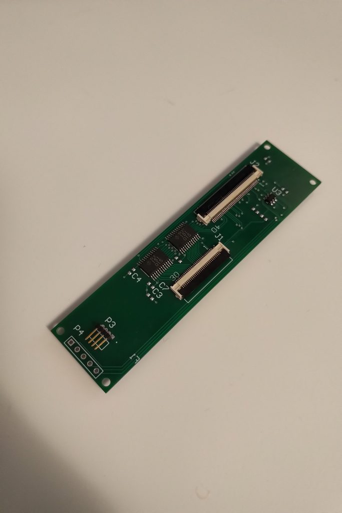
The issue I described as “blue tint” turns out to have been a fault in my test system. I built another revision of the PCB including pads for capacitors, and it would seem I only needed to place a cap on the clock line to resolve the remaining signal integrity issues.
Current Status
Full VGA Clock (25.175MHz) without any pixel errors / artifacts
Full brightness control via the contrast keys
Less than 100µA draw on the 10.5V inverter supply while display is off.
All electrical load is on the inverter supply wires and not the fpc.
250mA fuse to reduce risk of blowing the internal 650mA fuse in any unexpected failure modes.
Using the Hitachi transceivers maintains same electrical interface to the CT65535 as the OEM display. This may be an overkill step but it is working well so I am sticking with it.
Next Steps
Further verify there are no pixel errors at the higher clock speed.
Revise the PCB to simplify assembly and clean it up.
Update the 3d model for the new bezel to accommodate the new PCB.